No-μController EEPROM Reader
(2016) | 692 words (2 mins)
A few years ago I desoldered a 93C56 EEPROM from something I was salvaging parts from. I decided it would be interesting to test if I could use pushbuttons and LEDs in place of data lines from a microcontroller to read and write to and from the EEPROM.
About the 93C56 EEPROM
EEPROM stands for Electronically Erasable Programmable Read-Only Memory. As per its name, the contents can be written and erased using electrical pulses. This particular EEPROM has a capacity of 2048 bytes, or approximately 2KB. This is not a lot of memory in the context of the devices we use today. Even the smallest NES games typically ran around 8KB, and the image on this page is 170KB. However, EEPROMs find wide use where small volume, persistent storage is required. For example, an EEPROM could be used to store high scores on an arcade machine, or the mileage on a car.
Principle of Operation
The chip has four main pins relating to the operation in my circuit - the clock pin, the data in pin, the data out pin, and the Chip Select pin.
Integrated circuits are not continuously operating devices - every operation is performed to a beat. Sending pulses to the clock pin provides this beat. The data in and data out pins take and give out electrical pulses. Finally, the Chip Select pin wakes up the chip and tells it to be ready to work. This is useful because you can connect multiple chips to the same clock, data in and data out lines, and use the chip select to determine which one is to communicate at any given time. When multiple chips access the same data and clock lines at different times, the lines are commonly called a ‘bus’.
By sending different combinations of 1s and 0s (bits) to the data in over multiple clock pulses, you directly access various “commands” of the chip. The first few bits indicates the operation of the chip - commands like ‘read’, ‘write’ etc. The next few bits can be used to indicate an address to be accessed or data to be written.
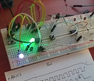
Circuit Development
I started by using a pushbutton for the Clock Pulse, a pushbutton for data in, a switch for Chip Select and an LED for data out. At first, I encountered issues because the pushbuttons created “bounce” - a phenomenon in which many pulses are received for a single button press. This is caused by the non-ideal contacts in the switch literally bouncing at a microscopic level before finally coming to rest in the pushed position. This was especially problematic for the clock line, where each press would actually trigger dozens of clock cycles. I decided instead to replace the clock button with a 555 timer. A low pass filter may have also solved the debounce issue, but I continued with the 555 timer circuit so I wouldn’t have to coordinate pushing more buttons than I had to. No debounce was required on the other buttons because the chip only reads from them on each rising edge of the clock pulse
Example
If the ‘read’ command is selected by sending the appropriate start bits, after clocking in the address you wish to read from (in binary, represented by the 1s and 0s on the data in line), the chip will output the binary for the data stored at that address, one bit at a time, over the next 8 clock pulses.
The following video explains the circuit and demonstrates a read, as outlined in the previous paragraph.
As for the circuit, here is the diagram.
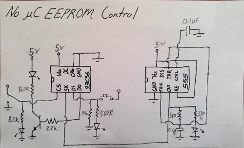
The circuit diagram. Note the 5M resistor… it’s not a very elegant circuit. At the time of making it I didn’t fully understand how to use the 555 timer chip.
At one byte per 30 seconds, this is obviously not a practical way to read or program an EEPROM! This project was done mostly to demonstrate how chips are interfaced with by microcontrollers, on a very slow time scale. Indeed, microcontrollers interface with these chips in the same way, albeit with electrical signals instead of pushbuttons and of course, much faster speeds.